Designing an e-paper badge from the case inward
Measure the parts first. The case will tell you the rest.
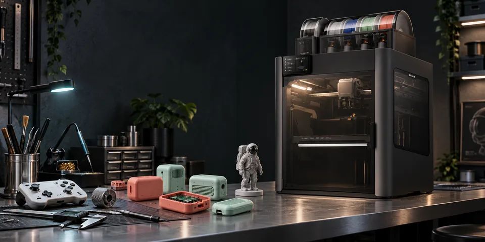
One of the projects on my bench is a compact e-paper badge: a small portrait tag you can hang on a lanyard, update over Bluetooth, and charge over USB-C, with a single button. It is the kind of gadget I mention on the physical side of the lab, and it is still early. So far it exists as measured parts, a CAD enclosure and a written plan with gates between stages.
I am writing it up at this point on purpose. Most of the decisions that shape a small device happen before anything is soldered, and they are easy to forget once the thing works.
The parts that set the size
The core is short:
- Seeed XIAO nRF52840 for the microcontroller. It has Bluetooth LE, an onboard USB-C port and a single-cell LiPo charger, which means one port can handle both flashing and charging.
- Waveshare 1.54-inch e-paper module, a 200 by 200 pixel black-and-white panel driven over SPI by an SSD1681 controller.
- A single-cell LiPo battery, size still to be decided.
- One compact tactile switch.
E-paper suits a badge because the image stays on the panel with the power off. A full refresh takes around two seconds and a partial refresh around 0.3 seconds, so the plan is to use partial updates for most changes and do a full refresh roughly every ten partials to clear ghosting. The firmware plan uses PlatformIO with the GxEPD2 display library and Adafruit’s Bluefruit library for Bluetooth.
Measuring before modelling
I modelled the case in Fusion 360 around the components’ STEP files and measured those models instead of trusting nominal drawings. Several numbers changed the design.
The display module’s board is 48.3 by 33.5 mm. Its panel face sits about 1.1 to 1.2 mm proud of that board over an area of roughly 32 by 42 mm, so the panel itself, not the board, is what a bezel can rest on. On the back, the 8-pin connector shroud stands 5.8 mm tall. Together with the battery, that shroud decides how thick the badge can be.
The mounting holes were also slightly off from where I expected. Nominally the top pair sits at plus and minus 14 mm across and 19.8 mm up from the centre of the active area. Measured, they were at 13.92 and minus 14.08 across and 19.69 up. That is about a tenth of a millimetre, which is enough for an alignment post to bind instead of dropping in. The posts are now centred on the measured holes.
Rev A to Rev B
The first layout stood the XIAO upright beneath the display with its USB-C port facing down. That worked on paper, but it meant the badge could not stand on its bottom edge while charging, and the area under the display came out 23.5 mm tall. The whole body was 67.5 mm.
Rev B rotates the XIAO by 90 degrees so the USB-C port exits the right edge. The connector face sits flush in its opening, recessed by 0.28 mm so it is never proud of the case. The section under the display shrank by about 4 mm, and the body is now 37.5 by 57.8 by 14.7 mm, or 63.3 mm tall including the lanyard loop. The XIAO’s antenna end sits in open space in the footer, away from the battery, which should help Bluetooth.
The protruding keyring nub from Rev A became an angled tag loop at the top-left corner with a racetrack-shaped slot through it, closer to the reference look I wanted.
Snaps, ledges and clamps
The front shell has a 28 by 28 mm window. An inner ledge rests on the panel face, so the display cannot fall out of the front and the e-paper sits about a millimetre behind the bezel. Two alignment posts go through the module’s mounting holes to stop it rotating, and the closed back sandwiches everything in place.
The back cover closes with five cantilever hooks. Each beam is 5 mm wide and 1.2 mm thick, with a barb that engages about 0.8 mm and a 0.5 mm lead-in chamfer so the cover slides closed and holds on a square catch face. All the catch pockets are blind, which keeps the outside of the case clean. In Rev A, I reused the left-side pocket coordinates on the right wall. Because the body is not symmetrical, those pockets broke through the outer skin. Rev B rebuilt the right side properly.
The XIAO needs more than locating. Its USB-C port has to line up with an opening that leaves only about 0.3 mm around the connector, so the board is clamped on all six faces, with measured gaps between 0.05 and 0.23 mm. The front shell and back cover together come to roughly 12.5 g of PLA.
For printing, the plan is test parts in PETG or foamed PLA, then final parts in PLA Matte or PETG on my Bambu Lab H2C with a 0.4 mm nozzle, 0.2 mm layers and four wall loops. I expect to tune the snap-fits by about a tenth of a millimetre after the first test print.
When the checker says zero
The most useful lesson so far came from the interference check. It first reported zero clashes. That result was wrong: the filter compared bodies by identity, and the proxy objects it was comparing never matched. After switching to comparing stable entity tokens and checking bodies in pairs, it found a real clash of 5.96 cubic millimetres between the registration lip and a clamp feature, which I then fixed in the model.
A clean result from a check you have not tested is not much evidence. I now treat a surprising zero the same way I treat a surprising failure.
Decisions still open
Four decisions are written down with a recommendation each, and none are locked yet:
- Board architecture. A custom carrier board with the XIAO soldered on keeps its USB-C port and charger, which is the low-risk path. A fully custom board with a bare nRF52840 module would be smaller, with more design work.
- Display. Keeping the Waveshare module avoids designing the display’s drive circuit. Using the raw panel with a 24-pin flex connector and the SSD1681 boost circuit on my own board would be thinner.
- Battery. A 250 mAh cell measuring 25 by 20 by 6 mm, which the current enclosure is packed around, or a larger protected 600 mAh cell. The XIAO has a charger but no discharge protection, so the cell needs protection either way.
- The button. My preference is one switch for everything: short press to cycle screens, long press to pair, and a very long hold to put the nRF52840 into its deepest sleep, where it draws around 0.4 microamps until a press wakes it.
Stages with gates
The plan has four stages, and each one ends with a gate that has to pass before I spend money on the next. The first is a breadboard prototype with firmware; it passes when an image pushed over Bluetooth renders on the display and sleep current measures in microamps. The second is a custom PCB, written in atopile, laid out in KiCad and fit-checked against the enclosure as a 3D model before ordering. The third revises the enclosure around the real board and battery. The fourth checks the charging path, the materials and a full cycle of charge, push, render, sleep and wake.
The gates exist because small hardware projects tend to skip ahead. Ordering boards before the firmware loop works, or printing final parts before the battery is chosen, would just mean doing the work twice.
 Talk to me on LinkedIn